Assuming that for a paramagnetic material, the magnetic susceptibility is inversely proportional to temperature in Kelvin, obtain Curie-Weiss law for the paramagnetic phase of a ferro-magnetic material.
20 Marks
Assuming that for a paramagnetic material, the magnetic susceptibility is inversely proportional to temperature in Kelvin, obtain Curie-Weiss law for the paramagnetic phase of a ferro-magnetic material.
Draw the circuit of an emitter-follower and find its voltage gain.
Simplify the following logic function and draw the corresponding logic gates: Y = A.B + B.\overline{C} + \overline{A}.B + \overline{A}.C + \overline{B}.\overline{C} + \overline{A}.\overline{B}.\overline{C} + A.B.C
Explain the basic distinction between a perfect conductor and a superconductor.
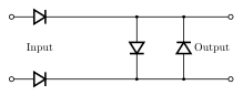
Four silicon diodes are connected as shown in Fig. 1. A sinusoidal voltage of amplitude 2\text{ V} is applied in the input. What is the waveshape of the output and its amplitude? If the amplitude of the input voltage is reduced to 1\text{ V}, what will be the waveshape of the output and its amplitude ? Threshold voltage of each diode is 0.6\text{ V}.
Define ex-OR. Give its truth table and draw the possible logic blocks.
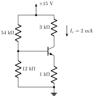
A Si BJT is connected as shown Fig . Show that it is in active region and works as an amplifier Calculate its mid frequency gain, given that BJT has h_{ie} = 1\text{ k}\Omega, h_{oe} = h_{re} = 0, I_{co} = 20\text{ nA}.
Derive the expression for the frequency spectrum of a carrier wave of frequency f_c which is amplitude modulated by a frequency f_m. A certain transmitted radiates 9\text{ kW} of power when the carrier wave is unmodulated and 10.12\text{ kW} power when the carrier wave is sinusoidally modulated. Calculate the modulation index.
Establish the two Barkhausen conditions for sustained sinusoidal oscillations. Sketch the circuit of Wien's bridge oscillator and explain its working.
Draw the block diagram of a superhetro dyne radio receiver and explain the function of local oscillator.
How does build in potential appear across a p-n junction? Explain under what biasing conditions drift and diffusion currents, respectively, dominate.
Derive an expression for magnetic susceptibility below Neel's temperature for a ferromagnetic substance.
Explain the construction and working of a p -n junction solar cell.
What is the difference between the frequency spectrum of amplitude modulated wav and frequency modulated waves? Give a circuit for the detection of frequency modulated waves.
Draw a circuit using AND, OR and NOT gate to realize the following truth table: \begin{array}{|c|c|c|c|} \hline \multicolumn{3}{|c|}{\text{INPUTS}} & \text{OUTPUT} \\ \hline A & B & C & Y \\ \hline 0 & 0 & 0 & 0 \\ 0 & 0 & 1 & 1 \\ 0 & 1 & 0 & 1 \\ 1 & 0 & 0 & 1 \\ 0 & 1 & 1 & 0 \\ 1 & 0 & 1 & 0 \\ 1 & 1 & 0 & 0 \\ 1 & 1 & 1 & 1 \\ \hline \end{array}
Describe the characteristics of grounded emitter transistor amplifier circuit and determine expression for (i) Input resistance (ii) Output resistance (iii) Current gain (iv) Voltage gain (v) Power gain
Describe and explain the theory and operation of the Zener diode. Explain what is meant by (i) Avalanche breakdown (ii) Zener breakdown
Explain ferrimagnetism. How is it different from antiferromagnetism?
Show that in the non-degenerate approximation the Fermi level in an n-type semiconductor is slightly below the bottom of the conduction band and in p-type it is slightly above the top of the valence band, but in both cases it remains within the band gap.
Write a short note on superconductivity.